Note: You must be registered in order to post a reply. To register, click here. Registration is FREE!
T O P I C R E V I E W
Sarath Chandran
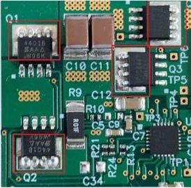
Posted - 30 Apr 2021 : 15:04:37 Hi, I wish to add a copper area behind few components for the heat dissipation purpose as highlighted in the attached image (behind Q1,Q2,Q3 etc) . How can I do that in Pulsonix?
Image Insert: 43.04 KB
3 L A T E S T R E P L I E S (Newest First)
Sarath Chandran
Posted - 04 May 2021 : 10:51:32 Thanks a tonne both for your valuable suggestions, I will try this.
jameshead
Posted - 30 Apr 2021 : 15:34:00 Insert Template and create a template that is the same size or larger than the area you wish to use for heat dissipation. Select the template, then right-click and select ADD TO NET. Select the net that the pins for the SOICs are being connected to. Select the template and pour it. Use Insert Shape to draw a rectangle, or whatever shape you want, on the relevant Solder Mask layer for the area that you want to be exposed. If you use a Polygon rather than a rectangle you need to make sure that it is closed. Then select this shape, click the right mouse button, and fill it.
bkamen
Posted - 30 Apr 2021 : 15:29:38 There are a few ways.
If the pins are isolated and just need to be soldered to something, then you could
* Use a copper shape -- add it to the net of the pins needing heat dissipation and then
Or
* Make a copper pour template, connect it to the net of the pins and pour. Although this can be a little more tricky since you'll have to watch the pour order of your template when re-pouring a whole board or make sure to pour it first and then lock all the poured copper.
Or
* You could make the extra copper part of the device footprint.
Also, don't forget you can use lots of vias to connect to copper on the opposite side of the PCB although keep in mind Vias have their thermal charasteristics. A copper pad on the same side of the chip will be better than a pad on the other side of the PCB with insufficient vias to pipe the heat.
I have a Samsung monitor designed this way - and it has thermal problems with the audio amp where the designers didn't follow the datasheet layout guidelines and didn't supply enough heat dissipation or on the same side as the chip AND they parked other components (alum capacitors) too close to the audio amp which ultimately causes these 2 caps to fail and the audio to go wonky.