Our PCB manufacturer has sometimes remarks about the plating index and show us pictures that give an impression of overplating / underplating in some parts of the PCB. Does Pulsonix have a tool to check the plating before we sent our data to the manufacturer.
There is a report 'Copper Per Layer' which can provide data for the designer to use to help them achieve a suitable index. The layers can be viewed against each other in the package and within independent viewers.
Copper areas can be cross-hatched or filled in a variety of forms and copper area can be added to help balance if required.
Ultimately it will be the board manufacturer who will check that the balance of copper is suitable for their processes and advise, but the designer can be proactive in their design of the board and thus ensure a good copper balance is initially provided.
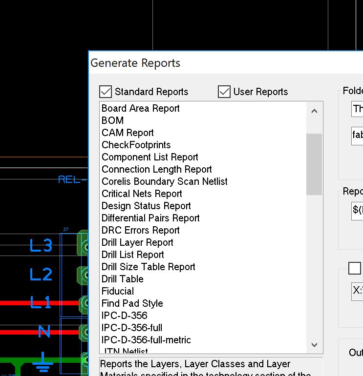
Ok, that sounds good, but where can i find the 'Copper by layer' report ? When i look in the reports i can generate i don't see a 'Copper by layer' choice.