
Advanced Technology Features
Leading Edge Technology for today's modern designs
Essential functionality to support Chip-On-Board technology
Chip-On-Board Technology
Chip-On-Board
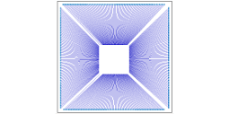
The Chip-On-Board option provides features for creation and annotation of die & bond pads and bond wires. It also allows automatic placing bond pads around the die. Within the Pulsonix design the bond pads are treated as special pads and can move independently of die and normal pads.
Advanced Rule Sets
Pulsonix contains a set of rules that are obeyed using both the Online DRC and batch DRC processes. Rules can be set for min and max length of the bond pad from the die pad, and for the crossing over of bond wires. Conditional Spacing rules can be defined for COB devices that use smaller values for this type of detailing. This is also a highly desirable requirement where mixed conventional and bare die technologies are used.
Component Interaction
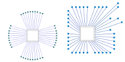
Components which contain die and bond pads are handled intelligently using an advanced rule set. Bond pads can be interactively moved independently of the main die 'body'. This movement is controlled using the min and max length rules of the bond wire, with cross-over rules also maintained in this process. The chip die can also be moved independently of the bond pads and position reset if needed.
Data Migration
Pulsonix delivers the largest collection of free Import Filters available in the industry. Import Schematic and PCB Designs as well as the Libraries from your current system; retain your Intellectual Property with accuracy and precision.
And where an import filter for your product is not available, please contact us to discuss other options, such as rebuilding your designs from Gerber data and reverse engineering the PCB back into a working Schematic design to match!

Discover why thousands of companies around the world choose Pulsonix
"Pulsonix has provided us with maximum value through advanced software that is used in the engineering design department."
Andreas Sauer - Hoffmann+Krippner