Edit the part and check the tab marked "Pins" to see if you have added a netname to certain pins, then check the footprint to see if you have assigned a default netname to the pads.
It may be the case that you have entered netnames in the part, where pin 5 is netname VCC, and other pins have different netnames, whereas in the footprint you have assigned pin 5 to a numbered netname, which is also used by a different pad in the footprint.
Eg, Footprint has netname 3 for pin 3 and pin 5 Part has netname mynet for pin 3 and VCC for pin 5.
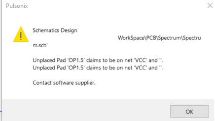
I removed my netnames to nothing and it did not help. I tried to delete the part from the schematic and synchronise designs, I still got the error, but a different one. See the picture.
Image Insert: 12.66 KB
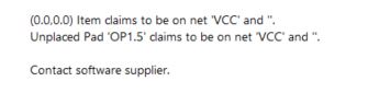
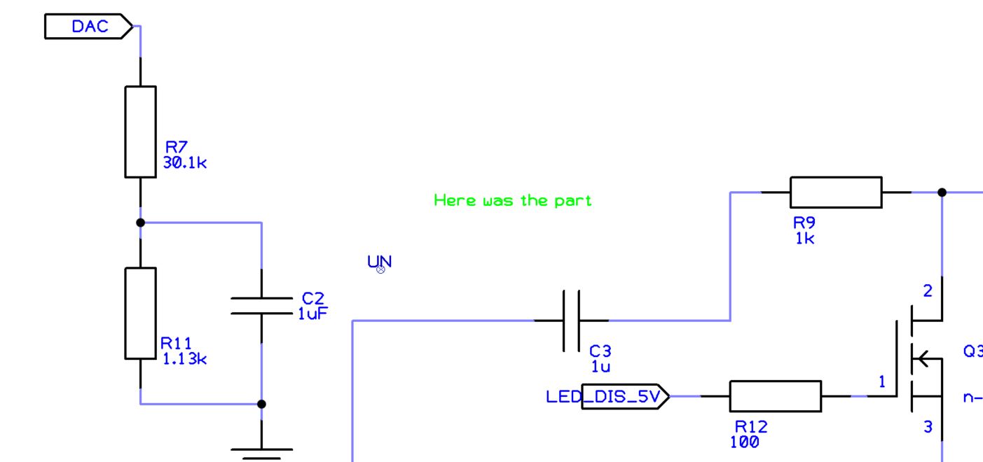
Then I tried to run the electrical rule check with the deleted part. I got error "Error : Unfinished Net (UN) 'VCC' on Ungated Pin OP1.5 near (111620.0,125846.0) on 'LED Driver'. " And it shows an error on some ghost part.
Image Insert: 52.97 KB
It is strange, that deleting the part did not help.