we are having an issue with via tenting. For a high density board we have epoxy filled and capped vias (IPC 4761 type VII) that we want completely covered with solder resist.
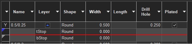
Adjusting the Styles > Pad in the PCB technology file, we used the "by layer" exception to reduce the pad size on top solder and bottom solder to 0.000. However, when we generate gerber plots, the solder mask layers retain solder mask openings that seem to correspond to the drill holes of the vias.
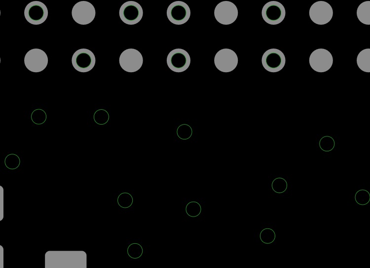
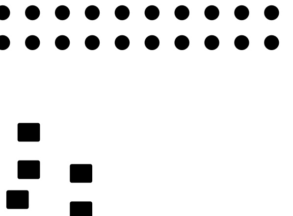
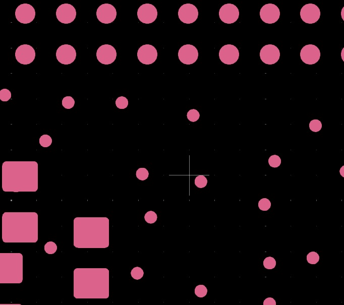
In the PCB window, when only the solder mask layer is displayed, only green circles are shown for the drills. In the gerber plot preview window, no solder mask is shown on the vias. But when viewing the generated Gerber files, the solder mask openings are there on the vias. I'll upload some pics to visualize.
Would much appreciate any pointers on removing these solder mask opening! :)
Pad Definitions: 26.56 KB
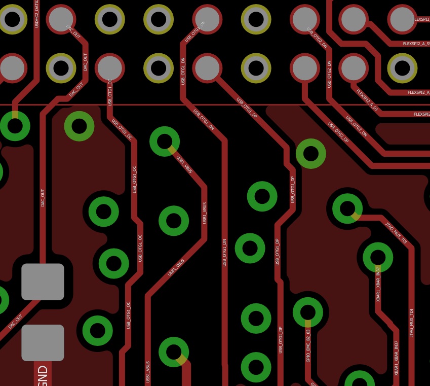
PCB window showing top layer: 157.36 KB
PCB window showing top solder mask layer: 32.69 KB
Gerber plot preview: 20.98 KB
Generated gerber data for solder mask layer: 40.12 KB
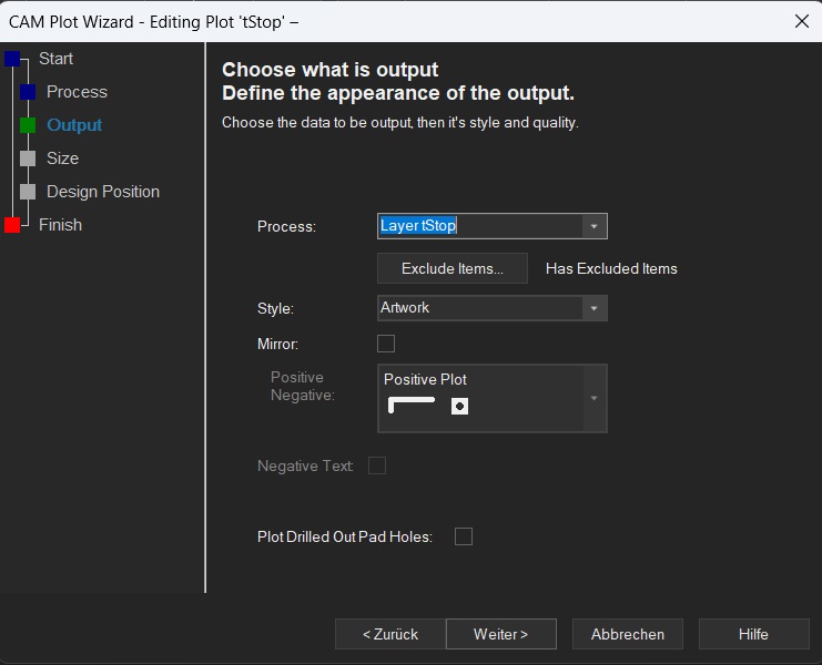
Under CAM/Plot you need to edit the solder mask plot using "Edit..." which opens the CAM Plot Wizard.
Click through the screens to "Output" and there is a checkbox "Plot Drilled Out Pad Holes". It was checked. After unchecking it, the tenting works properly.
@Pulsonix: If this setting could be shown in the cam plot settings table, that would be fabulous.